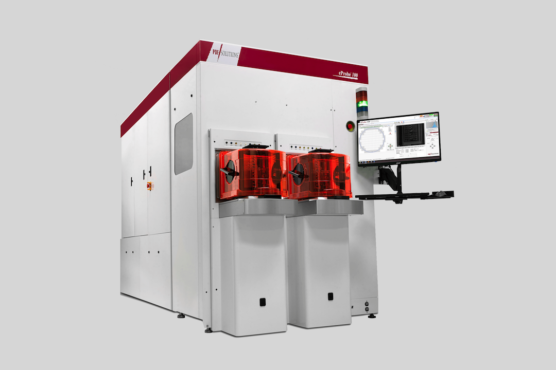
Gigamat
Hybrid Wafer Sorter for Semiconductor Manufacturing
Challenge
Develop a flexible hybrid wafer sorter and metrology system integrating best-in-class components from multiple suppliers. The system required advanced measurement capabilities, comprehensive factory automation, and production-level throughput—all delivered on an aggressive 7-month timeline.
Solution
Modular software architecture enabling parallel development and future scalability. Advanced metrology integration with dual resistivity and thickness measurements. Complete SECS/GEM factory automation interface. Precision coordination of 26 motion axes across robotic handlers, gantries, and measurement stations.
Impact
Achieved a 7-month delivery for a fully functional production system — cutting the typical 18–24 month timeline by more than half. Delivered 300+ wafers/hour throughput while maintaining measurement flexibility. Created scalable foundation enabling rapid adaptation for future GigaMat products and customer applications.

"The customer is very excited. They couldn't have gotten this system from anyone else. It's a huge advantage for them."

Engineering Flexibility at Scale in Semiconductor Manufacturing
By Edmond Abrahamians - President and CEO of GigaMat, Steve Ball - Staff Software Engineer at JKI and Sarah Zalusky - JKI Partner and Staff Project Engineer
In the $600 billion semiconductor industry, creating custom wafer manufacturing systems remains a formidable and often cost-prohibitive challenge. GigaMat met this challenge by partnering with JKI to develop a hybrid wafer sorter and metrology system, integrating best-in-class components from global suppliers, and delivering a production system which still provides flexibility.
JKI brought deep semiconductor expertise and a systematic approach to deliver the control software for this system on an aggressive seven month timeline
"We needed a ready-made software development team with the right skills and a can-do attitude. JKI delivered that and more." -- Edmond Abrahamians, President and CEO of GigaMat

The Challenge: Complexity Under Pressure
In semiconductor manufacturing, wafer sorting is a critical early-stage process. Before wafers can move to polishing and other fabrication steps, they must be grouped (or rejected) according to specific characteristics. GigaMat's system automatically measures incoming wafers and sorts them into output cassettes based on user-defined criteria.
"What makes our system unique is its flexibility and the custom selection of measurement devices," explains Abrahamians. "While the primary function is thickness-based sorting for production, we've integrated additional measurement capabilities that allow for more sophisticated sorting criteria and even a metrology-like operation.” To support this flexibility in production operation the system required an intelligent application, capable of orchestrating multiple precision systems, complex wafer handling operations, and a comprehensive factory interface, all while maintaining production-level throughput and reliability. The software also needed to be delivered on a very compressed development schedule, adding to the complexity of the project.
Solution Overview
Advanced Metrology
- Dual resistivity measurements using both contactless and 4-point probe methods
- Dual thickness measurements to enable precise wafer characterization
- Integrated conductivity type testing (P/N) for material verification
- Precision wafer alignment ensures accurate metrology across all samples
Factory Automation & Integration
- Extensive SECS/GEM interface enables seamless factory-level automation
- Custom equipment front end module (EFEM) developed for enhanced integration
- Complete wafer tracking system with RFID reader integration
- Full-featured operator GUI with interlocking and intuitive user layout
High-Performance Operation
- Supports high-throughput production sorting at 300+ wafers per hour
- Flexible measurement mode enables detailed wafer analysis when required
- Rigorous software interlocking across all components for safe operation
- Embedded safety controller manages complex interlocks and system states
Precision Wafer Handling
- Coordination of 26 motion axes across multiple robotic and gantry subsystems
- Multiple robotic handling systems integrated within the EFEM
- Precision gantries, elevators, and wafer pre-alignment stations
- Synchronized movement across all wafer measurement stations
The Gigamat semiconductor metrology system required advanced software capable of orchestrating a complex set of operations across four critical technical domains. From enabling cutting-edge measurement capabilities to managing seamless integration within a high-volume manufacturing environment, the solution demanded precision, adaptability, and reliability. JKI’s engineering team addressed these challenges through robust support for advanced metrology, comprehensive factory integration, multi-modal operation, and precision wafer handling.
Advanced Metrology
The system featured sophisticated metrology capabilities, including dual resistivity measurement using both contactless and 4-point probe technologies. Multiple measurement stations were employed for high-accuracy wafer thickness characterization, complemented by P/N type testing. Real-time data processing enabled immediate decision-making for wafer sort criteria, ensuring high-quality output and operational efficiency.
Comprehensive Factory Integration
To ensure seamless operation within a highly automated fab environment, JKI implemented a robust SECS/GEM interface and integrated the system fully with the factory’s Equipment Manager (EM) software. Wafer tracking was managed via multi-cassette RFID systems, and operators were supported with a comprehensive graphical user interface featuring intuitive workflows and safety interlocking.
Multi-Modal Operation
The software supported multiple operational modes, including high-throughput production sorting capable of processing more than 300 wafers per hour, flexible measurement modes for in-depth wafer analysis, and precise calibration routines. Each mode leveraged dynamic recipe configuration and enforced complex safety interlocks across the system to ensure safe, accurate, and efficient operation.
Precision Wafer Handling
The system coordinated 26 independent motion axes across robotic handlers, gantries, elevators, and pre-alignment and measurement stations. Handling required management of 15 critical wafer hand-off points with sub-millimeter accuracy and strict timing constraints. Real-time orchestration ensured seamless, concurrent operation of all subsystems, delivering high throughput without compromising precision.
"Integrating all these components was like conducting an orchestra," explains Steve Ball, Staff Software Engineer at JKI. "Every element had to move in harmony to achieve the desired results."
The integration complexity, high performance demands while preserving operational flexibility and the aggressive timeline, presented a significant challenge.

gigamat sorter inner view
JKI's Approach: Rapid Development Through Experience and Teamwork
"This amount of software development for such a complex system would have taken years with the resources we had in-house," notes Abrahamians.
JKI's approach leveraged deep experience in semiconductor manufacturing systems to accelerate development. "Because we've built similar systems, we could quickly architect a solution and lay out a project roadmap that would meet immediate needs and set a foundation for future systems," explains Sarah Zalusky, JKI Partner and Staff Project Engineer.
For a system of this complexity, industry standards would typically allocate 18-24 months for software development alone. JKI compressed this into seven months (from beginning engagement to beginning of Factory Acceptance Testing) while maintaining rigorous quality standards required for semiconductor manufacturing equipment. This exceptional timeline was achieved through a strategic three-pronged approach focused on architecture, processes, and implementation.
Architecture
A modular software architecture was developed from the ground up to serve as the foundation for this project and future GIGAMAT systems. The architecture was designed to support layered development, beginning with low-level hardware control components and building upward toward complex, coordinated system behaviors. This structured approach ensured scalability, maintainability, and consistent performance across subsystems.
Processes
The development process leveraged our modular architecture, enabling multiple engineering resources working on distinct system components in parallel. Working in parallel with a consistent architecture ensured seamless integration and accelerated delivery. A key aspect of the process included ongoing collaboration with the end customer to define and implement a comprehensive remote interface that ensured seamless factory integration. After core automation features were delivered, a focused phase targeted throughput optimization to meet high-volume production requirements.
Implementation
The implementation strategy prioritized validation of the foundational hardware control components before layering on higher-level functionality. A user-friendly graphical interface was designed to streamline operator interaction, enhance usability, and ensure safe, efficient system operation. This phased and user-centered approach enabled rapid system bring-up and ease of adoption on the manufacturing floor.

gigamat sorter user interface
Results: Speed, Flexibility, and Scalability
JKI delivered a system that not only met GigaMat's immediate needs but also provided a foundation for future development in just seven months—an aggressive timeline that required overcoming significant technical complexity and coordination challenges. Despite the time constraints, the team achieved a system throughput exceeding 300 wafers per hour while preserving the flexibility needed for detailed measurement and characterization.
Key accomplishments included the development of a robust SECS/GEM interface, enabling seamless integration with factory automation systems, and the successful coordination and control of a wide array of hardware components across the system. Additionally, the team implemented a flexible, modular software architecture designed to support future enhancements and adaptation, laying the groundwork for scalability and long-term maintainability.
A Partnership for Future Innovation
The successful delivery of the hybrid wafer sorter and metrology system represents more than just meeting an aggressive timeline – it demonstrates how technical expertise and thoughtful architecture can transform challenging requirements into lasting value.
"We have the framework now," Abrahamians explains. "When you have this foundation for the code, it makes it easy to develop other products."
The modular software architecture JKI developed allows GigaMat to quickly adapt the system for different customers and applications, turning what began as a time-critical project into a strategic advantage. In an industry where precision, speed, and flexibility are paramount, this collaboration between GigaMat and JKI shows how the right partnership can deliver both immediate solutions and long-term competitive advantages.

gigamat.com

JKI is a National Instruments Certified Silver Alliance Partner.

Seamless SECS/GEM Factory Integration with HUME Integration Software.

JKI is a Xilinx Alliance Program Associate.
Download the PDF to print it and share it with your colleagues.
Hybrid Wafer Sorter for Semiconductor Manufacturing
Building A Next-Generation Scanning Electron Microscope to Streamline Semiconductor Manufacturing
If you liked the "Hybrid Wafer Sorter for Semiconductor Manufacturing" Case Study you should also check out our "Scanning Electron Microscope for Semiconductor Tool" Case Study.