


Wafer Layout + Alignment
Achieve high-precision wafer metrology and inspection by leveraging intuitive wafer layout software and accurate machine vision alignment.

Automated Wafer Inspection
Empower your custom inspection IP with a high-throughput, fully-automated process. Define, execute, and manage test data to run inline during semiconductor manufacturing.

Fab Integration
Quickly integrate your system into Fabs using standard semiconductor factory automation software and protocols. Do you use PEER Group's PTO™ software? We do too!

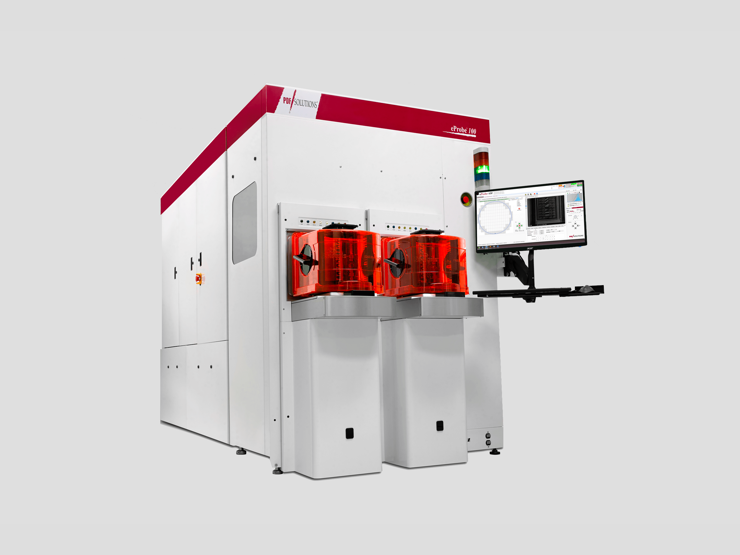
Next-Generation Scanning Electron Microscope
JKI worked with PDF Solutions to develop the control software for an inspection tool that can rapidly perform wafer metrology and help semicon companies streamline their manufacturing process.

Non-Destructive Wafer Inspection
Using JKI's tools and services allowed FemtoMetrix to field a fully operational wafer-defect detection system at a production semiconductor fab on a very aggressive schedule.


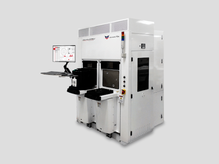
Hybrid Wafer Sorter for Semi Mfg
JKI worked with GigaMat to deliver a fully functional production grade - very high throughput hybrid wafer sorter - in 7 months (instead of the typical 18-24 months).


Yoram Schwarz
Director of Software Engineering, PDF Solutions

